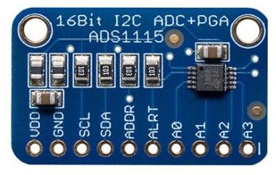
Module – ADS1115 – 4-Channel 16-Bit ADC Module
Hardware
Informatie (ENG)
Description
The ADS1115 device is a precision, low-power, 16-bit, I2C-compatible, analog-to-digital converters (ADCs) offered in an ultra-small, leadless, X2QFN-10 package, and a VSSOP-10 package. The device incorporates a low-drift voltage reference and an oscillator. The converter also incorporates a programmable gain amplifier and a digital comparator. These features, along with a wide operating supply range, make the converter well suited for power- and space-constrained, sensor measurement applications.
The ADS1115 perform conversions at data rates up to 860 samples per second (SPS). The PGA offers input ranges from ±256 mV to ±6.144 V, allowing precise large- and small-signal measurements. The converter features an input multiplexer that allows two differential or four single-ended input measurements. Use the digital comparator in the ADS1115 for under- and overvoltage detection.
The ADS1115 operates in either continuous-conversion mode or single-shot mode. The devices are automatically powered down after one conversion in single-shot mode; therefore, power consumption is significantly reduced during idle periods.
Features
Wide Supply Range: 2.0 V to 5.5 V
Low Current Consumption: 150 µA
(Continuous-Conversion Mode)
Programmable Data Rate: 8 SPS to 860 SPS
Single-Cycle Settling
Internal Low-Drift Voltage Reference
Internal Oscillator
I2C Interface: Four Pin-Selectable Addresses
Four Single-Ended or Two Differential Inputs
Programmable Comparator
Operating Temperature Range: –40°C to +125°C
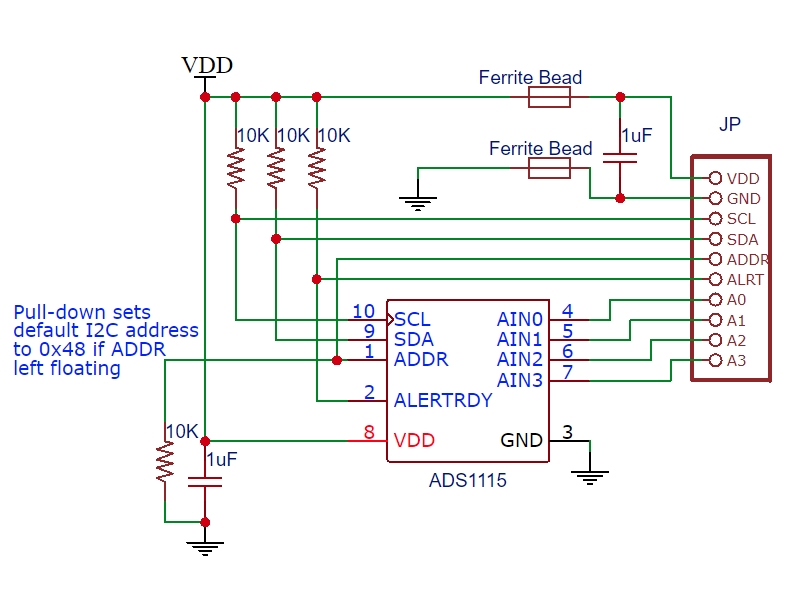
I2C Interface
The module has an easy to use I2C interface that can be configured to use any one of four different I2C addresses if you want to use multiple modules in the same system or if you run into an address conflict with another device..
The ADDR address pin determines which I2C address to use by connecting it as follows:
- 0x48 = ADDR connected to Ground
- 0x49 = ADDR connected to VDD
- 0x4A = ADDR connected to SDA
- 0x4B = ADDR connected to SCL
Input Modes
The 4 inputs can be configured to operate in 3 different modes.
Single-Ended Mode
In single-ended mode, the 4 inputs (Ao-A3) can each be used as separate inputs with each referenced to ground. This mode provides more inputs, but have less electrical noise rejection and provides 15-bits of resolution.
Differential Mode
In differential mode of operation, the inputs act in pairs to measure the difference in voltage between the two inputs. The channel pairing is A0 – A1 and A2 – A3. This mode provides differential noise immunity which may be important in some critical measurement situations when very small signals are being measured or there is a lot of electromagnetic noise pickup.
Since the measurement is relative to each other, the full 16-bits of resolution are available.
You will sometimes see it stated that the differential mode allows you to measure negative voltages, but this is somewhat misleading. No inputs on this device can be negative relative to ground or the device will be damaged. What it means is that one of the differential inputs can be negative relative to the other differential input, but they will both be positive voltages relative to ground. See the section below about measuring negative voltages for more info on this.
Comparator Mode
In comparator mode, the input is constantly measured and compared against a value that has be set in the device. When the signal exceeds the predefined value, the ALRT pin is activated LOW. This pin can be polled by a MCU or it can be used to drive an interrupt. The board includes a 10K pull-up on this line.
Measurement Range
The ADS1115 is a 16-bit device, but in single-ended mode the output is a signed integer and one of the bits is used for the sign so in practice it is providing 15-bits of resolution which means there are 32,767 steps of resolution.
The maximum voltage that can be measured and thus the size of the steps of resolution is controlled by the Programmable Gain Amplifier (PGA). The PGA has 6 full-scale ranges that can be set as shown in the table below.
| Full Scale Range | LSB (Step) Size |
| 6.144 V | 187.5uV |
| 4.096 V | 125uV |
| 2.048 V | 62.5uV |
| 1.024 V | 31.25uV |
| 0.512 V | 15.625uV |
| 0.256 V | 7.8125uV |
The default setting of the PGA is set for the maximum range of 6.144V. This provides a resolution step size of 6.144V / 32767 steps = 187.5uV. This is a much smaller step size than the standard Arduino ADC which provides about 4.88mV per step.
Keep in mind that the absolute maximum voltage that can be measured is VDD + 0.3V. If the device is operating at 5V, the maximum voltage that can be safely measured is 5.3V. The range above that that is basically wasted. If higher voltages then the maximum are input, the device can be damaged.
If the voltages to be measured are smaller and it is desired to optimize the resolution of the reading, the PGA can be programmed to have a full range down to as small as 0.256V which gives a resolution of 7.8125uV per step.
Important Note: If using the device to measure the voltage across a shunt resistor using differential mode, ensure that the 5.5V maximum voltage of the ADS1115 device is not being exceeded. While the voltage being measured across the shunt may be very small, if the shunt is on the high side of the load in a 12V circuit for instance, the voltage relative to ground will far exceed the rating of the device. Typically a shunt must be on the low side of a load for this device to be used.
Conversion Modes
Continuous Conversion Mode:
The module normally operates in continuous conversion mode. In this mode, the ADS1115 is constantly performing conversions. If a read is made, the last conversion that was completed will be reported.
Single-Shot Mode
The device draws little power, but if you are looking for minimum power draw, the ADS1115 can be put into single-shot mode. In this mode, the conversion is only run when requested and then the device goes back into a low power mode. The Alert/Ready pin can optionally be used to determine when the conversion has been completed.
Measuring Negative Voltages
A common point of confusion when using this device is that the spec sheet gives the full scale range in both positive and negative numbers such as ±6.144. This makes it easy to think that the device can measure both positive and negative voltages relative to ground, but that is not the case. Any negative voltage relative to ground > -0.3V will damage the device.
The ± is only applicable to the differential mode of operation. With the A0/A1 differential pair for instance, the A0 input is considered the positive input and A1 is the negative input. Both inputs must have positive voltages applied to them, but if the voltage on A0 is larger than A1, the difference between them is reported as a positive number while if A1 is larger than A0, the result is reported as a negative number.
For example, if you connect a battery across the two inputs with the positive lead connected to A0 and negative lead to A1, the voltage will be reported as +1.5V. If you then reverse the battery, the voltage will be reported as -1.5V. Similarly if A0 is connected to +2V and A1 is connected to +3V, the measurement will be -1V.
If you application requires the measurement of voltages that are negative relative to ground, you will need to provide an offset to make it a positive voltage for measurement.
Module Assembly
This module comes with the header loose. This allows you to configure the module to meet your particular requirements such as which side of the board you want the header on or if you want to solder on wires to make the connections. For use with breadboards, we put the headers on the bottom so that the module can plug directly into the breadboard.
Module Connections
The connections to the module are straight forward.
- Supply 3.3 or 5V power and ground
- Connect I2C SCL and SDA lines to same on the MCU. The ADDR and ALRT lines can be ignored for now.
- Connect the voltage to be measured to the analog input(s). Be sure to observe the requirement not to exceed the VDD voltage on the analog inputs.
Pinout
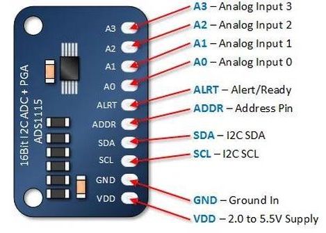
- VDD = VDD (2.0V – 5.5V) typically connects to MCU 3.3V or 5V
- GND = Ground connects to MCU ground
- SCL = I2C SCL connects to MCU I2C SCL
- SDA = I2C SDA connects to MCU I2C SDA
- ADDR = I2C Address. Default if left unconnected is 0x48.
- ALRT= Alert / Ready. Alert output for comparator or Ready output for conversion complete in single-shot mode
- A0 = Analog input 0
- A1 = Analog input 1
- A2 = Analog input 2
- A3 = Analog input 3
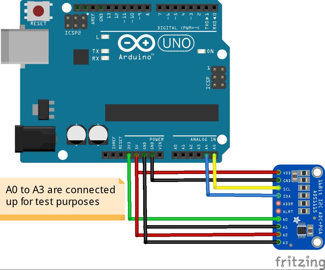
Arduino
Sluit de module aan volgens onderstaand schema.
Script
Needed: Adafruit ADS1015 library @ https://github.com/adafruit/Adafruit_ADS1X15
|
1 2 3 4 5 6 7 8 9 10 11 12 13 14 15 16 17 18 19 20 21 22 23 24 25 26 27 28 29 30 31 32 33 34 35 36 37 38 39 40 41 42 43 44 45 46 47 48 |
/* ADS1115 4-Ch 16-bit ADC Test Program Basic code to test the ADS1115 ADC Module. Takes a single-ended reading on module channel A0. Uses default measurement range of of 6.144V Module connections: VDD = 5V Gnd = Ground SCL = SCL / A5 on uC SDA = SDA / A4 on uC ADDR = Board has pull-down to ground (sets I2C address of 0x48) A0 = 3.3V on uC. Voltage to be measured. Can be any voltage < 5V Uses Adafruit ADS1X15 library which can be downloaded via IDE */ #include <Wire.h> #include <Adafruit_ADS1015.h> Adafruit_ADS1115 ads(0x48); // Create ads object at default I2C address float Voltage = 0.0; // Voltage reading from ADS1115 //=============================================================================== // Initialization //=============================================================================== void setup() { ads.begin(); // Initialize ads <b>Serial</b>.begin(9600); // Set comm speed for serial monitor window } //=============================================================================== // Main //=============================================================================== void loop() { int16_t adc0; // Return value from ADC is 16-bit integer adc0 = ads.readADC_SingleEnded(0); // Take a single-ended reading on A0 channel Voltage = (adc0 * 0.1875)/1000; // Convert raw reading into a voltage <b>Serial</b>.print("A0 Reading: "); <b>Serial</b>.print(adc0); // Print raw reading <b>Serial</b>.print("\tVoltage: "); <b>Serial</b>.println(Voltage, 7); // Print calculated voltage out to 7 digits <b>Serial</b>.println(); delay(1000); // Take a reading every second } |
Bron(nen):
http://arduinolearning.com/amp/code/ads1115-analog-to-digital-converter-and-arduino.php
Raspberry Pi
Sluit de module aan volgens onderstaand schema.

Standaard heeft deze module I2C adres 0x48:
|
1 2 3 4 5 6 7 8 9 10 |
i2cdetect -y 1 0 1 2 3 4 5 6 7 8 9 a b c d e f 00: -- -- -- -- -- -- -- -- -- -- -- -- -- 10: -- -- -- -- -- -- -- -- -- -- -- -- -- -- -- -- 20: -- -- -- -- -- -- -- -- -- -- -- -- -- -- -- -- 30: -- -- -- -- -- -- -- -- -- -- -- -- -- -- -- -- 40: -- -- -- -- -- -- -- -- 48 -- -- -- -- -- -- -- 50: -- -- -- -- -- -- -- -- -- -- -- -- -- -- -- -- 60: -- -- -- -- -- -- -- -- -- -- -- -- -- -- -- -- 70: -- -- -- -- -- -- -- -- |
Script
Library: https://github.com/adafruit/Adafruit_Python_ADS1x15
Adafruit_Python_ADS1x15-master (DL @ 2020-12-18)
Install the Adafruit ADS1115 library for ADC
With the update done, we are now ready to install the dependencies starting with the Adafruit python module for the ADS115 chip. Ensure you are in the Raspberry Pi home directory by running;
|
1 |
<strong>cd ~</strong> |
then install the build-essentials by running;
|
1 |
<strong>sudo apt-get install build-essential python-dev python-smbus git</strong> |
Next, clone the Adafruit git folder for the library by running;
|
1 |
<strong>git clone </strong><a href="https://github.com/adafruit/Adafruit_Python_ADS1x15.git" target="_blank" rel="nofollow noopener"><strong>https://github.com/adafruit/Adafruit_Python_ADS1x15.git</strong></a> |
Change into the cloned file’s directory and run the setup file;
|
1 2 |
<strong>cd Adafruit_Python_ADS1x1z </strong> <strong>sudo python setup.py install</strong> |
After installation, your screen should look like the image below:

Test the library and 12C communication.
Before we proceed with the rest of the project, it is important to test the library and ensure the ADC can communicate with the raspberry pi over I2C. To do this we will use an example script that comes with the library.
While still in the Adafruit_Python_ADS1x15 folder, change directory to the examples directory by running;
|
1 |
<strong>cd examples</strong> |
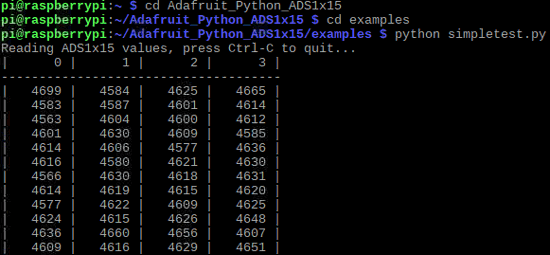
Next, run the sampletest.py example which displays the value of the four channels on the ADC in a tabular form.
Run the example using:
|
1 |
<strong>python simpletest.py</strong> |
If the I2C module is enabled and connections good, you should see the data as shown in the image below.
|
1 2 3 4 5 6 7 8 9 10 11 12 13 14 15 16 17 18 19 20 21 22 23 24 25 26 27 28 29 30 31 32 33 34 35 36 37 38 39 40 41 42 43 44 45 46 47 48 49 50 51 52 53 |
# Simple demo of reading each analog input from the ADS1x15 and printing it to # the screen. # Author: Tony DiCola # License: Public Domain import time # Import the ADS1x15 module. import Adafruit_ADS1x15 # Create an ADS1115 ADC (16-bit) instance. adc = Adafruit_ADS1x15.ADS1115() # Or create an ADS1015 ADC (12-bit) instance. #adc = Adafruit_ADS1x15.ADS1015() # Note you can change the I2C address from its default (0x48), and/or the I2C # bus by passing in these optional parameters: #adc = Adafruit_ADS1x15.ADS1015(address=0x49, busnum=1) # Choose a gain of 1 for reading voltages from 0 to 4.09V. # Or pick a different gain to change the range of voltages that are read: # - 2/3 = +/-6.144V # - 1 = +/-4.096V # - 2 = +/-2.048V # - 4 = +/-1.024V # - 8 = +/-0.512V # - 16 = +/-0.256V # See table 3 in the ADS1015/ADS1115 datasheet for more info on gain. GAIN = 1 print('Reading ADS1x15 values, press Ctrl-C to quit...') # Print nice channel column headers. print('| {0:>6} | {1:>6} | {2:>6} | {3:>6} |'.format(*range(4))) print('-' * 37) # Main loop. while True: # Read all the ADC channel values in a list. values = [0]*4 for i in range(4): # Read the specified ADC channel using the previously set gain value. values[i] = adc.read_adc(i, gain=GAIN) # Note you can also pass in an optional data_rate parameter that controls # the ADC conversion time (in samples/second). Each chip has a different # set of allowed data rate values, see datasheet Table 9 config register # DR bit values. #values[i] = adc.read_adc(i, gain=GAIN, data_rate=128) # Each value will be a 12 or 16 bit signed integer value depending on the # ADC (ADS1015 = 12-bit, ADS1115 = 16-bit). # Print the ADC values. print('| {0:>6} | {1:>6} | {2:>6} | {3:>6} |'.format(*values)) # Pause for half a second. time.sleep(0.5) |
Bron(nen):
https://circuitdigest.com/microcontroller-projects/raspberry-pi-based-oscilloscope
http://www.getmicros.net/ads1115-analog-to-digital-converter-and-raspberry-pi-example-in-c.php
Schema
Teardown
GEEN GEGEVENS
Datasheet
Fritzing
Downloads
GEEN GEGEVENS