EMC – Rekening houden met EMC tbv printplaat ontwerp
![]()
Elektromagnetische straling en interventie van componenten op een PCB is niet fijn en kan voorkomen worden als men het ontwerp aanpast en/of diverse componenten toevoegd, learnemc.com heeft daarvoor een aantal tutorials en tips beschikbaar gesteld: http://learnemc.com/pcb-layout
Video voorbeelden: youtube.com
PCB Layout
Some circuit designs are fabricated on tiny silicon wafers and others consist of various components connected by cables. However, the circuits that are often the center of an EMC engineer’s attention are those that are laid out on fiberglass epoxy boards. Printed circuit boards similar to the one illustrated in Figure 1 can be found in nearly all electronic systems. Circuit components with metal pins are connected by copper traces. Surface mount technology (SMT) components are glued to the top and/or bottom of a board. Pin-in-hole components are held to the board by their pins, which extend through the board and are soldered to the traces on the opposite side.
Single-layer boards have all of the traces routed on one side of the board. Double-layer boards have traces on both sides. Many boards have several layers of copper traces separated by layers of fiberglass epoxy (or a similar dielectric). These are referred to as multi-layer boards. The number of layers is usually even. Four-layer boards are very common in low-cost products. Boards with dozens of layers are sometimes used to connect densely populated boards with high component pin counts.
Multi-layer boards usually have entire layers with solid copper planes dedicated to the distribution of power to the components on the board. These planes are usually named after the component pins they are connected to. For example, a copper plane connecting all of the VCC components pins to the power supply is often called a VCC plane.
The placement of components and the routing of traces usually play a crucial role in determining the electromagnetic compatibility of products employing printed circuit boards. Well laid out boards will not radiate significantly on their own and they do a good job of minimizing currents and fields that might couple noise to cables or other objects off the board. They also are configured to minimize opportunities for external currents or fields to couple interfering signals on to the board.
Printed Circuit Board Design Guidelines
As indicated earlier in these notes, many board designers employ a list of guidelines to help place components and route traces. Now that we know a little more about noise sources, antennas and coupling mechanisms on printed circuit boards, we can take a closer look at some of these design guidelines and understand why and when they are important. Below is a list of 16 EMC design guidelines for printed circuit boards along with a short justification for each.
1. The lengths of traces carrying high-speed digital signals or clocks should be minimized.
High-speed digital signals and clocks are often the strongest noise sources. The longer these traces are, the more opportunities there will be to couple energy away from these traces. Remember also, that loop area is generally more important than trace length. Make sure that there is a good high-frequency current return path very near each trace.
2. The lengths of traces attached directly to connectors (I/O traces) should be minimized.
Traces attached directly to connectors are likely paths for energy to be coupled on or off the board.
3. Signals with high-frequency content should not be routed beneath components used for board I/O.
Traces routed under a component can capacitively or inductively couple energy to that component.
4. All connectors should be located on one edge or on one corner of a board.
Connectors represent the most efficient antenna parts in most designs. Locating them on the same edge of the board makes it much easier to control the common-mode voltage that may drive one connector relative to another.
5. No high-speed circuitry should be located between I/O connectors.
Even if two connectors are on the same edge of the board, high-speed circuitry located between them can induce enough common-mode voltage to drive one connector relative to the other resulting in significant radiated emissions.
6. Critical signal or clock traces should be buried between power/ground planes.
Routing a trace on a layer between two solid planes does an excellent job of containing the fields from these traces and prevents unwanted coupling.
7. Select active digital components that have maximum acceptable off-chip transition times.
If the transition times of a digital waveform are faster than they need to be, the power in the upper harmonics can be much higher than necessary. If the transitions times of the logic employed are faster than they need to be, they can usually be slowed using series resistors or ferrites.
8. All off-board communication from a single device should be routed through the same connector.
Many components (especially large VLSI devices) generate a significant amount of common-mode noise between different I/O pins. If one of these devices is connected to more than one connector, this common-mode noise will potentially drive a good antenna. (The device will also be more susceptible to radiated noise brought in on this antenna. )
9. High-speed (or susceptible) traces should be routed at least 2X from the board edge, where X is the distance between the trace and its return current path.
The electric and magnetic field lines associated with traces very near the edge of a board are less well contained. Crosstalk and coupling to and from antennas tends to be greater from these traces.
10. Differential signal trace pairs should be routed together and maintain the same distance from any solid planes.
Differential signals are less susceptible to noise and less likely to generate radiated emissions if they are balanced (i.e. they have the same length and maintain the same impedance relative to other conductors).
11. All power (e.g. voltage) planes that are referenced to the same power return (e.g. ground) plane, should be routed on the same layer.
If, for example, a board employs three voltages 3.3 volts, 3.3 volts analog and 1.0 volt; then it is generally desirable to minimize the high-frequency coupling between these planes. Putting the voltage planes on the same layer will ensure that there is no overlap. It will also help to promote an efficient layout, since the active devices are unlikely to require two different voltages at any one position on the board.
12. The separation between any two power planes on a given layer should be at least 3 mm.
If two planes get too close to each other on the same layer, significant high-frequency coupling may occur. Under adverse conditions, arcing or shorts may also be a problem if the planes are too closely spaced.
13. On a board with power and ground planes, no traces should be used to connect to power or ground. Connections should be made using a via adjacent to the power or ground pad of the component.
Traces on a connection to a plane located on a different layer take up space and add inductance to the connection. If high-frequency impedance is an issue (as it is with power bus decoupling connections), this inductance can significantly degrade the performance of the connection.
14. If the design has more than one ground plane layer, then any connection to ground at a given position should be made to all of the ground layers at that position.
The overall guiding principle here is that high-frequency currents will take the most beneficial (lowest inductance) path if allowed to. Don’t try to direct the flow of these currents by only connecting to specific planes.
15. There should be no gaps or slots in the ground plane.
It’s usually best to have a solid ground (signal return) plane and a layer devoted to this plane. Any additional power or signal current returns that must be DC isolated from the ground plane should be routed on layers other than the layer devoted to the ground plane.
16. All power or ground conductors on the board that make contact with (or couple to) the chassis, cables or other good “antenna parts” should be bonded together at high frequencies.
Unanticipated voltages between different conductors both nominally called “ground” are a primary source of radiated emission and susceptibility problems.
In addition to the 16 guidelines above, board designers often employ guidelines that are specific to their industry. For example, “Clock generation circuits employing phase-locked loops should have their own isolated power derived from the board’s power through a #1234 ferrite bead. ” These guidelines based on experience can be invaluable to the knowledgeable board designer. However, these same guidelines applied to other designs with no concept of where they came from or why they work can result is wasted effort and non-functional boards. It is very important to understand the basic physics behind each and every guideline being applied.
It is also important to identify the potential noise sources, antennas and coupling paths with every single design you evaluate. The best design won’t be the one that complies with the most guidelines. The best design is the one that meets all of the specifications with the lowest cost and highest reliability.
Example 1: A Simple One-Layer Board Layout
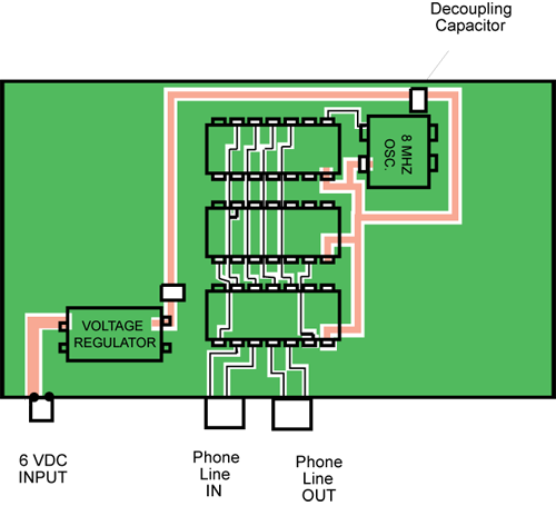
Harvey invents a device that keeps a record of the telephone calls made from his phone. The design is relatively simple and is shown in Figure 15. However, when it is hooked up to the phone line, radiation from the device interferes with his TV reception.
Redesign Harvey’s board in order to reduce the radiated EMI. You may move components and/or add components, but you must use a single-sided board.

We should begin by identifying the potential sources and antennas. Certainly, the 8-MHz clock signal is a potential source and so are the data lines. This device may also put significant noise on the power traces. Potential antenna parts are the three connectors. Nothing else on this board is large enough to be an efficient radiation source.
When we start to rearrange the components, we should try to put all of the antenna parts (i.e. the connectors) on one side of the board. We should also reorient the components to minimize the length of the traces. Finally, we should fill the empty space on the board with ground and make sure that each signal trace has a nearby return path.
One solution to this problem is shown in Figure 16. Try to trace the path of the 8-MHz signal current in the layout of Figure 15 compared to the same path in Figure 16. This current flows out the clock output pin of the oscillator, into the clock input pin of the upper IC, out the ground pin of the upper IC, and into the ground pin of the oscillator. This loop area is significantly smaller in the Figure 16 layout. Also note that no high-frequency current returns on the portion of the plane between any two connectors in the Figure 16 layout.
The design in Figure 15 is unlikely to meet a radiation emissions specification and therefore cannot be marketed or sold. The design in Figure 16 should meet virtually any country’s radiated emissions specification without the need for any shielding or high-cost components. Note that we could have provided pads for mounting filter components on the phone lines if we felt that might be necessary.