IC – TDA2822 – Dual Power Amplifier
Hardware
Source: https://components101.com/ics/tda2822-dual-power-amplifier
The TDA2822 is a dual low power audio amplifier in an 8-Pin plastic dual in-line package. This IC comes with features like low crossover distortion, low quiescent current, and supply voltage range of this IC is 3V to 15V.
TDA2822 Audio amplifier features and specifications
- Supply Voltage: 3-15V
- Output Power: 3.2 W
- Audio – Load Impedance: 8 Ohms
- Gain: 39 dB
- Operating Supply Current: 12 mA
- Ib – Input Bias Current: 0.1 uA
- PSRR – Power Supply Rejection Ratio: 40 dB
- Available in 8-Pin DIP package
Equivalent for TDA2822: C4556C, NJM4560
Alternatives Audio Amplifiers: LM386, AD620, IC6283, JRC45558
Where to use TDA2822 Amplifier IC
The TDA2822 is a Dual Audio Amplifier IC, meaning it has two Op-Amps inside its package, and they are commonly used for audio amplification because of their wide bandwidth gain. The two outputs can deliver 250 milliwatts output power. This IC can be used in portable audio systems, preamplifiers, hearing aid mini radio, headphone amplifier, etc.
So if you are looking for a dual package Operational amplifier IC with high-gain, and wide bandwidth for audio amplification, then this IC might be the right choice for you.
Applications of TDA2822 Amplifier
- AM and FM Radio amplifiers
- Portable music players
- Low Power Audio amplifiers
- Wien bridge oscillator
- Power Amplifiers
- Audio boosters
Pinout
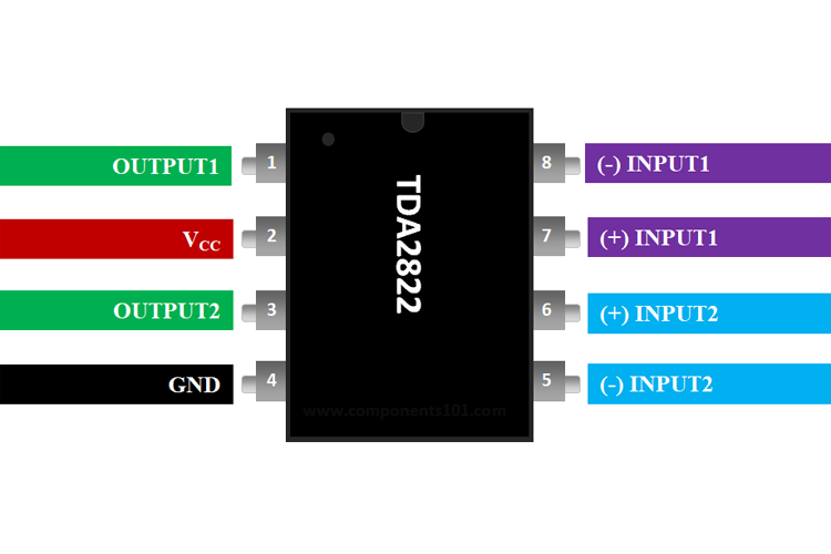

TDA2822 Pinout Configuration
| Pin Number | Pin Name | Description |
| 1,3 | Output | Provides the amplified Audio output |
| 5,8 | Inverting Input (IN-) | The Inverting Pin of an amplifier is normally grounded |
| 6,7 | Non-Inverting Input (IN+) | The Non-Inverting pin is provided with the audio signal |
| 4 | Vcc- | Connected to the negative supply rail |
| 2 | Vcc+ | Connected to Positive Supply Rail |
Schema
How to use TDA2822 Amplifier
An application circuit for stereo from TDA2822 datasheet is given below
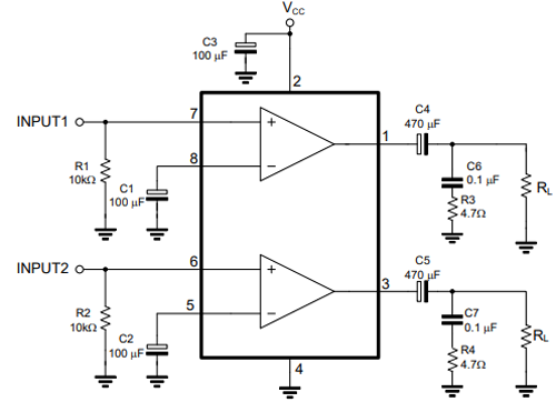
The left load is connected to output pin 1 of the IC through electrolytic capacitor C4, and the right load is connected to output pin 3 through electrolytic capacitor C5. The Inverting Input Pins (5 and 8) are connected to the ground via electrolytic capacitors. Non-Inverting Input Pins (7 and 6) are connected to input1 and input2. Pin 2 is connected to DC supply and pin 4 is connected to ground. Electrolytic capacitor C3 connected across VCC and ground, work as a filter capacitor.
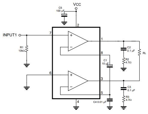
In the datasheet you can also find the bridge MONO schematic, wich is more powerfull: